
- 18 Oct 2025
- ⚙ Coding Vibes
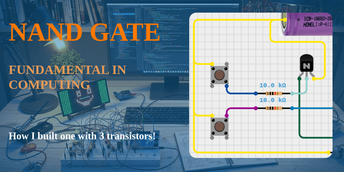
During my college, the lowest level of computing I studied were the logic gates. It's closely linked to boolean algebra and they are the fundamental part of any computer. Nowadays, I wanted to explore deeper into electronics. In order to hone my skills, I started out my venture by trying to build a logic gate: the NAND gate!
Bear with me as I walk you through the theory, conception and the end result.
Why a NAND gate
The NAND gate (Not-AND) is the foundational component of nearly all digital electronics. Why? Because it’s a universal gate—meaning you can build every other logic gate (NOT, AND, OR, XOR, etc.) using only NAND gates.
Even more fascinating is how simple the core circuit is. We can demonstrate the power of the NAND function using just three active switching components: three transistors.
The logic results is should produce
Our NAND gate will take 2 inputs which can be HIGH or LOW (0 or 1). The output of the NAND gate is practically a HIGH or LOW. Basically, it will return LOW (0) when both inputs are HIGH (1). Here's the logic table:
| Input A | Input B | NAND Result |
| 0 (LOW) | 0 (LOW) | 1 (HIGH) |
| 0 (LOW) | 1 (HIGH) | 1 (HIGH) |
| 1 (HIGH) | 0 (LOW) | 1 (HIGH) |
| 1 (HIGH) | 1 (HIGH) | 0 (LOW) |
Overview
The basic NAND function requires two distinct actions:
- The AND part: The output signal is held LOW only if both inputs are HIGH.
- The NOT part: The entire AND result must be inverted.
We achieve this by connecting two switching transistors (Q1 and Q2) in a series configuration, which performs the AND function, and using the third transistor (Q3) as a final inverter (NOT gate).
Besides the transistors, we also have a couple of resistors whose role is to limit the current to the transistors base and also act as pull up resistors. I still struggle a bit with the concept of pull-up resistors, you can read more about them here, I think it's explained pretty well. Tried a lot of combinations of resistors before settling down to this configuration ⭐.
The components that I used
Let's also mentioned the list of components that you need to create such a NAND gate.
- Battery: for this configuration I used 3.3V (1 piece)
- Transistors: NPN transistors, model 2N 5551, many other types can be used (3 pieces)
- Resistors: necessary to limit current and ensure stable digital output (5 in total)
- 10K - 2 pieces
- 1K - 1 piece
- 2.2K - 1 piece
- 68K - 1 piece
- Push buttons: in order to simulate HIGH or LOW (2 pieces)
- LED: see the digital output, 1 - LED on, 0 - LED off (1 piece)
- Breadboard: stable base of building (1 piece)
- Wires: general purpose Dupont wires (lots of pieces)
Now over the internet, I found different values for the resistors and also slight modifications of the circuit. I'm not saying they are flawed, they should work, but in my case this configuration worked flawlessly! Try it out, it should work fine for you as well!
The schema of the circuit
After I got the circuit working on my breadboard, I also created its design in Cirkit Designer. This also helps me to keep track of the inner workings, especially the resistor sizes. Here's how it looks like:
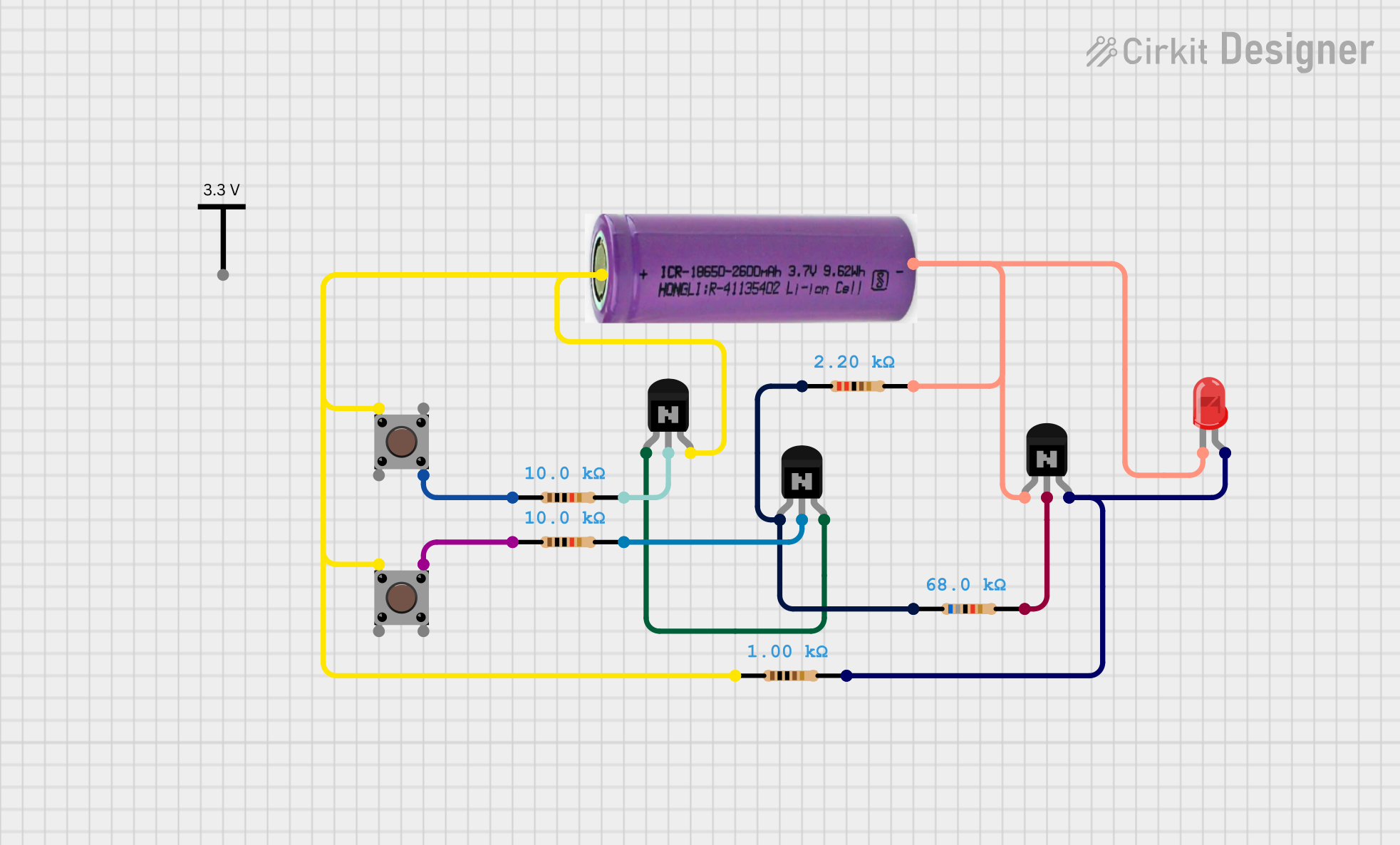
Remember the battery is a 3.3V. The yellow line represents the Vcc and brick red line the ground. The transistors are NPN with pins from right to left: Collector, Base, Emitter. They are set up in order Q1, Q2, Q3.
Let's explain the wiring a bit:
- The Vcc from the battery feeds directly into:
- The collector of Q1
- Push button 1
- Push button 2
- 1K transistor which connects to the collector of Q3 and the anode of the LED (plus signal)
- The output part of both inputs go to the bases of Q1 and Q2 respectively via 10K resistors. They are necessary to limit the current of the base, which should be less than the collector's in order for the transistor to work correctly
- The emitter of Q1 goes directly to the collector of Q2
- Then the emitter of Q2 has 2 bifurcations:
- One to the GND via the 2.2K resistor
- One to the base of Q3 via the 68K resistor. I'll explain below why a larger resistor
- Finally, the emitter of Q3 goes directly to the GND, ensuring a fast escape path for the current when Q3 transistor is saturated. And of course the LED cathode to the GND to close the circuit properly
Breaking it down
Let's assume we have this circuit ready and plugged in. It should immediately turn the LED on because no current flows through the inputs. The current flows through the 1K resistor to the collector of Q3, Q3 cuts off since its base is 0. This wiring is also connected to the LED hence immediately turns ON.
If we press the button 1, then another path of the current flows through the 10K through the base of Q1. Q1 is then emitting a current to Q2. Q2 does not emit onwards since its base is 0. The other part of the circuit flows like before so LED stays ON.
If we also press the button 2, then Q2 also starts emitting current, part of it goes to GND through the 2.2K resistor and the other part goes through the 68K resistor to the Q3's base. Q3 will saturate and let pass almost all the current from the collector through it directly to GND, practically depleting the LED of powers. The LED turns OFF. At this stage there's still some current flowing through the LED, but not enough for it to get bright.
The last scenario is when just button 2 is pressed and current passes through it. To me it was tricky because in my first circuit configuration, it did not turn off the LED completely, just dimmed it.That happened because emitter of Q2 was directly connected to base of Q3. This impeded the Q3 transistor to act properly as a switch allowing quite a reasonable amount of current to flow into the LED just enough to make it bright. After a couple of tries, I noticed that a large enough but not too large resistor like the one of 68K did the trick. This ensured that Q3 properly saturates and becomes an easy escape route for the current in this scenario. Another thing to consider is that also Q2 needs a resistor to GND so that Q3 doesn't accidentally saturate.
If you want to see it in action, watch my YouTube video.
Conclusion
There you have it, the basis of computing in the palm of your hands! I'm excited to be able to build such a thing. For most people, it might seem trivial, but for me it was quite a learning journey with trial and error. Really grateful for what I learned and hope it's going to be helpful for you as well!
Let me know if you have any remarks, questions or other ideas! Cheers ✨